Discussion:
FPGA motherboard for 80386 CPU
(too old to reply)
Rick C. Hodgin
2017-11-10 15:35:36 UTC
Permalink
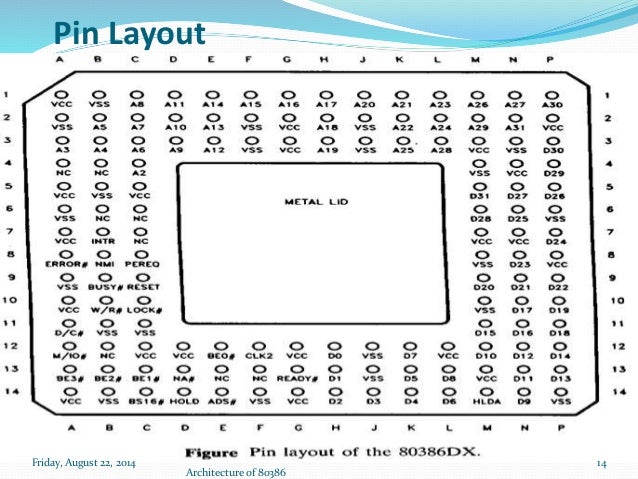
The 80386DX CPU had 132 pins:

80386DX and 80386SX pinouts:
Loading Image...
Loading Image...

General architecture:
http://www.nptel.ac.in/courses/Webcourse-contents/IISc-BANG/Microprocessors%20and%20Microcontrollers/pdf/Teacher_Slides/mod8/M8L1.pdf

Of these pins on the DX variant:

32 pins -- data
30 pins -- address
4 pins -- byte enables in 32-bit writes
1 pin -- Read/write
1 pin -- Data/Control
1 pin -- Memory/IO
1 pin -- Bus mastering lock issued by CPU
1 pin -- Bus16 size (16-bit when asserted, normally 32-bit)
1 pin -- Next address (for pipelining)
1 pin -- Address valid signal
--
73 pins -- For basic I/O

3 pins -- Math-coprocessor support
1 pin -- Ready (or Wait, for bus cycles to complete)
2 pins -- Hold and Hold Acknowledge (for bus mastering)
2 pins -- Interrupt and Non-masktable Interrupt
--
8 pins -- General coordination with external peripherals

1 pin -- Reset
1 pin -- Double-pumped clock
--
2 pins -- System input

The rest of the pins are unused, go to VSS or VCC. This means that for a
full 80386 "motherboard" only 83 pins are required to fully support its
operation, 67 of which are address, data, and data type, leaving really
only 15 pins of complex operation for a state machine.

-----
Would anybody be able to help me create this 80386 motherboard using an
AMD Am386 CPU, which is a static CPU operating from 0 to 40 MHz? I would
like to get it working with a single-step operation for design validation,
and then to begin ramping it up.

I figure I'll have an area of ROM which the CPU boots to load, which is a
tiny real mode program, which begins computing something that can be exam-
ined by the FPGA to test successful operation. And then move on to more
complex operations, including a custom microkernel.

--
Rick C. Hodgin
rickman
2017-11-10 19:46:26 UTC
Permalink
Post by Rick C. Hodgin
http://www.rfwireless-world.com/images/80386-pin-diagram.jpg
https://image.slidesharecdn.com/salientfeatursof80386-140822084001-phpapp02/95/salient-featurs-of-80386-14-638.jpg?cb=1408709884
http://www.nptel.ac.in/courses/Webcourse-contents/IISc-BANG/Microprocessors%20and%20Microcontrollers/pdf/Teacher_Slides/mod8/M8L1.pdf
32 pins -- data
30 pins -- address
4 pins -- byte enables in 32-bit writes
1 pin -- Read/write
1 pin -- Data/Control
1 pin -- Memory/IO
1 pin -- Bus mastering lock issued by CPU
1 pin -- Bus16 size (16-bit when asserted, normally 32-bit)
1 pin -- Next address (for pipelining)
1 pin -- Address valid signal
--
73 pins -- For basic I/O
3 pins -- Math-coprocessor support
1 pin -- Ready (or Wait, for bus cycles to complete)
2 pins -- Hold and Hold Acknowledge (for bus mastering)
2 pins -- Interrupt and Non-masktable Interrupt
--
8 pins -- General coordination with external peripherals
1 pin -- Reset
1 pin -- Double-pumped clock
--
2 pins -- System input
The rest of the pins are unused, go to VSS or VCC. This means that for a
full 80386 "motherboard" only 83 pins are required to fully support its
operation, 67 of which are address, data, and data type, leaving really
only 15 pins of complex operation for a state machine.
-----
Would anybody be able to help me create this 80386 motherboard using an
AMD Am386 CPU, which is a static CPU operating from 0 to 40 MHz? I would
like to get it working with a single-step operation for design validation,
and then to begin ramping it up.
I figure I'll have an area of ROM which the CPU boots to load, which is a
tiny real mode program, which begins computing something that can be exam-
ined by the FPGA to test successful operation. And then move on to more
complex operations, including a custom microkernel.
I'm sure many here would be *able* to help you. The question you should be
asking is who would be *willing* to help you...

What parts are you having trouble with? Why do you need help exactly?
--
Rick C

Viewed the eclipse at Wintercrest Farms,
on the centerline of totality since 1998
Rick C. Hodgin
2017-11-10 20:19:55 UTC
Permalink
Post by rickman
Post by Rick C. Hodgin
http://www.rfwireless-world.com/images/80386-pin-diagram.jpg
https://image.slidesharecdn.com/salientfeatursof80386-140822084001-phpapp02/95/salient-featurs-of-80386-14-638.jpg?cb=1408709884
http://www.nptel.ac.in/courses/Webcourse-contents/IISc-BANG/Microprocessors%20and%20Microcontrollers/pdf/Teacher_Slides/mod8/M8L1.pdf
32 pins -- data
30 pins -- address
4 pins -- byte enables in 32-bit writes
1 pin -- Read/write
1 pin -- Data/Control
1 pin -- Memory/IO
1 pin -- Bus mastering lock issued by CPU
1 pin -- Bus16 size (16-bit when asserted, normally 32-bit)
1 pin -- Next address (for pipelining)
1 pin -- Address valid signal
--
73 pins -- For basic I/O
3 pins -- Math-coprocessor support
1 pin -- Ready (or Wait, for bus cycles to complete)
2 pins -- Hold and Hold Acknowledge (for bus mastering)
2 pins -- Interrupt and Non-masktable Interrupt
--
8 pins -- General coordination with external peripherals
1 pin -- Reset
1 pin -- Double-pumped clock
--
2 pins -- System input
The rest of the pins are unused, go to VSS or VCC. This means that for a
full 80386 "motherboard" only 83 pins are required to fully support its
operation, 67 of which are address, data, and data type, leaving really
only 15 pins of complex operation for a state machine.
-----
Would anybody be able to help me create this 80386 motherboard using an
AMD Am386 CPU, which is a static CPU operating from 0 to 40 MHz? I would
like to get it working with a single-step operation for design validation,
and then to begin ramping it up.
I figure I'll have an area of ROM which the CPU boots to load, which is a
tiny real mode program, which begins computing something that can be exam-
ined by the FPGA to test successful operation. And then move on to more
complex operations, including a custom microkernel.
I'm sure many here would be *able* to help you. The question you should be
asking is who would be *willing* to help you...
What parts are you having trouble with? Why do you need help exactly?
The 80386DX was a 5V part. My FPGA supports 3.3V, so I need some
kind of level shifter? I'll need to build a breakout board to route
through my existing 40-pin FPGA breakout ports (160 pins). So, do
I go with an online custom manufacturer? Buy materials and pattern
and etch my own board, soldering everything myself? Are there generic
sockets the Am386 would fit in which are already broken out?

I need help with the mechanics of Verilog. I know how I want things
to route, but the mechanics of the language confuse me. I don't
understand why at times I need registers, and other times I can
route wires. The assignments are confusing me, when to use <= and
when not to, etc.

I need basic help to get my feet off the ground.

--
Rick C. Hodgin
rickman
2017-11-10 21:11:35 UTC
Permalink
Post by Rick C. Hodgin
Post by rickman
Post by Rick C. Hodgin
http://www.rfwireless-world.com/images/80386-pin-diagram.jpg
https://image.slidesharecdn.com/salientfeatursof80386-140822084001-phpapp02/95/salient-featurs-of-80386-14-638.jpg?cb=1408709884
http://www.nptel.ac.in/courses/Webcourse-contents/IISc-BANG/Microprocessors%20and%20Microcontrollers/pdf/Teacher_Slides/mod8/M8L1.pdf
32 pins -- data
30 pins -- address
4 pins -- byte enables in 32-bit writes
1 pin -- Read/write
1 pin -- Data/Control
1 pin -- Memory/IO
1 pin -- Bus mastering lock issued by CPU
1 pin -- Bus16 size (16-bit when asserted, normally 32-bit)
1 pin -- Next address (for pipelining)
1 pin -- Address valid signal
--
73 pins -- For basic I/O
3 pins -- Math-coprocessor support
1 pin -- Ready (or Wait, for bus cycles to complete)
2 pins -- Hold and Hold Acknowledge (for bus mastering)
2 pins -- Interrupt and Non-masktable Interrupt
--
8 pins -- General coordination with external peripherals
1 pin -- Reset
1 pin -- Double-pumped clock
--
2 pins -- System input
The rest of the pins are unused, go to VSS or VCC. This means that for a
full 80386 "motherboard" only 83 pins are required to fully support its
operation, 67 of which are address, data, and data type, leaving really
only 15 pins of complex operation for a state machine.
-----
Would anybody be able to help me create this 80386 motherboard using an
AMD Am386 CPU, which is a static CPU operating from 0 to 40 MHz? I would
like to get it working with a single-step operation for design validation,
and then to begin ramping it up.
I figure I'll have an area of ROM which the CPU boots to load, which is a
tiny real mode program, which begins computing something that can be exam-
ined by the FPGA to test successful operation. And then move on to more
complex operations, including a custom microkernel.
I'm sure many here would be *able* to help you. The question you should be
asking is who would be *willing* to help you...
What parts are you having trouble with? Why do you need help exactly?
The 80386DX was a 5V part. My FPGA supports 3.3V, so I need some
kind of level shifter? I'll need to build a breakout board to route
through my existing 40-pin FPGA breakout ports (160 pins). So, do
I go with an online custom manufacturer? Buy materials and pattern
and etch my own board, soldering everything myself? Are there generic
sockets the Am386 would fit in which are already broken out?
I don't follow what you are saying here. What is a 40 pin breakout port?
Are you talking about connectors on an FPGA board? I don't understand your
goals, so I can't help you figure out what you need to do. Are you trying
to make a board that will plug into the existing socket on a 386 motherboard?
Post by Rick C. Hodgin
I need help with the mechanics of Verilog. I know how I want things
to route, but the mechanics of the language confuse me. I don't
understand why at times I need registers, and other times I can
route wires. The assignments are confusing me, when to use <= and
when not to, etc.
I'm not a Verilog guy so I can't help you with that. I'm more of a VHDL guy.
Post by Rick C. Hodgin
I need basic help to get my feet off the ground.
What's wrong with keeping your feet on the ground?

We've had this conversation before. Every project starts with goals (user
requirements in a formal analysis) which need to be translated to design
requirements and finally detailed as an implementation. You tend to mix
those various levels without understanding you are doing that.

What are your goals exactly?
--
Rick C

Viewed the eclipse at Wintercrest Farms,
on the centerline of totality since 1998
Rick C. Hodgin
2017-11-10 22:14:17 UTC
Permalink
Post by rickman
What is a 40 pin breakout port?
Are you talking about connectors on an FPGA board?
The FPGA uses a high density 160-pin connection. You can buy an
add-on board which takes the high-density connection and breaks
it out to 4x 40-pin connectors (like IDE cables).
Post by rickman
Are you trying
to make a board that will plug into the existing socket
on a 386 motherboard?
I'm trying to create a board an Am386 CPU will plug in to, which
then makes my FPGA its motherboard. I will be the north bridge
(memory and high speed I/O like graphics) and south bridge (low
speed I/O like keyboard, mouse, timer, etc).
Post by rickman
We've had this conversation before. Every project starts with goals (user
requirements in a formal analysis) which need to be translated to design
requirements and finally detailed as an implementation. You tend to mix
those various levels without understanding you are doing that.
I know what I want. I tend to work in my head more than in formal
writings.
Post by rickman
What are your goals exactly?
(1) Get the board designed physically, and ordered or built.
(2) Assemble the board.
(3) Write the Verilog code to feed and respond to the CPU's needs.
(4) Write basic software to test and debug the design.
(5) Write real hardware for video, sound, network, keyboard, mouse,
etc., to create a little 80386-based system.

Thank you,
Rick C. Hodgin
rickman
2017-11-10 23:31:17 UTC
Permalink
Post by Rick C. Hodgin
Post by rickman
What is a 40 pin breakout port?
Are you talking about connectors on an FPGA board?
The FPGA uses a high density 160-pin connection. You can buy an
add-on board which takes the high-density connection and breaks
it out to 4x 40-pin connectors (like IDE cables).
Post by rickman
Are you trying
to make a board that will plug into the existing socket
on a 386 motherboard?
I'm trying to create a board an Am386 CPU will plug in to, which
then makes my FPGA its motherboard. I will be the north bridge
(memory and high speed I/O like graphics) and south bridge (low
speed I/O like keyboard, mouse, timer, etc).
Post by rickman
We've had this conversation before. Every project starts with goals (user
requirements in a formal analysis) which need to be translated to design
requirements and finally detailed as an implementation. You tend to mix
those various levels without understanding you are doing that.
I know what I want. I tend to work in my head more than in formal
writings.
If you want to work with people, they can't see what's in your head. You
need to write stuff down to get help.
Post by Rick C. Hodgin
Post by rickman
What are your goals exactly?
(1) Get the board designed physically, and ordered or built.
You need to define the board a lot better.
Post by Rick C. Hodgin
(2) Assemble the board.
(3) Write the Verilog code to feed and respond to the CPU's needs.
That will require the FPGA either allow the CPU access to a memory device or
some other way serve up data from RAM and/or ROM. Do you know what you want
for that?

What other types of I/O do you intend to provide? Are you familiar with the
entire interface of the 386 CPU? You will need to know every detail. To
design the equivalent of a motherboard you would do well to find a 386 PC/AT
technical reference manual or other schematic for a motherboard. They used
TTL logic and you can easily implement that in the FPGA.
Post by Rick C. Hodgin
(4) Write basic software to test and debug the design.
(5) Write real hardware for video, sound, network, keyboard, mouse,
etc., to create a little 80386-based system.
So you want a full computer in an FPGA other than the 386 CPU? You will
also need a BIOS which is not open source... unless someone has an open
source BIOS... I don't recall hearing of one.

So where are the parts you need help with?
--
Rick C

Viewed the eclipse at Wintercrest Farms,
on the centerline of totality since 1998
Rick C. Hodgin
2017-11-10 23:59:57 UTC
Permalink
Post by rickman
Post by Rick C. Hodgin
Post by rickman
What are your goals exactly?
(1) Get the board designed physically, and ordered or built.
You need to define the board a lot better.
As I see it, the CPU is a black box. I connect wires to it and
give it power and turn things on and off, and observe it turning
things on and off, all by protocol, and it doesn't need anything
else.

I route all pins to appropriate I/O on the FPGA, or Vcc, and then
I need to have simulated ROM at the boot address, which simulates
BIOS. And I just read the Am386 was a CMOS 3.3V part, so that removes
level shifters.

Since I am the motherboard, all my BIOS would need to do is setup
interrupt vectors for CPU-issued interrupts (0x0 through 0x1f),
and run some software that does something I have control over.

First thing I need to do is get help on board design and components.
I'm thinking a socket (Package: PGA-132) with pins routed to the
mated 40-pin breakouts I would assign on my FPGA. Of the 160 pins,
only so many are GPIO, so I would have that limitation on design.

I think I could do all that, but there are things I don't know.
Will I need capacitors? Resistors? Some kind of something to handle
electrical oddities? If not, then I assume making trace lines equal
is important, but not greatly at only 40 MHz.

On the FPGA, it would route address and data pins to logic identifying
memory and I/O, and read / write, responding appropriately, routing
certain memory to emulated ROM, the rest to on-FPGA SRAM emulating
DRAM.

It seems a simple physical design. Moderately complex logically.
And very exciting. :-)

--
Rick C. Hodgin
rickman
2017-11-11 03:15:54 UTC
Permalink
Post by Rick C. Hodgin
Post by rickman
Post by Rick C. Hodgin
Post by rickman
What are your goals exactly?
(1) Get the board designed physically, and ordered or built.
You need to define the board a lot better.
As I see it, the CPU is a black box. I connect wires to it and
give it power and turn things on and off, and observe it turning
things on and off, all by protocol, and it doesn't need anything
else.
Everything is a black box in that sense. The "protocol" is the part you
need to understand in detail.
Post by Rick C. Hodgin
I route all pins to appropriate I/O on the FPGA, or Vcc, and then
I need to have simulated ROM at the boot address, which simulates
BIOS. And I just read the Am386 was a CMOS 3.3V part, so that removes
level shifters.
I can't find anything that says it was 3.3 volt. Where did you read this?
Post by Rick C. Hodgin
Since I am the motherboard, all my BIOS would need to do is setup
interrupt vectors for CPU-issued interrupts (0x0 through 0x1f),
and run some software that does something I have control over.
Yes, if you don't plan to run it as a PC, but have you figured out any of this?
Post by Rick C. Hodgin
First thing I need to do is get help on board design and components.
I'm thinking a socket (Package: PGA-132) with pins routed to the
mated 40-pin breakouts I would assign on my FPGA. Of the 160 pins,
only so many are GPIO, so I would have that limitation on design.
Board design is not as hard at 40 MHz as at 100's of MHz, but you still need
to know something about signal integrity. If not sometimes the voltages
will bounce and jitter and so look like the wrong voltage when sampled and
clocks can bounce and double clock on a single edge. This is *very*
important stuff to know.
Post by Rick C. Hodgin
I think I could do all that, but there are things I don't know.
Will I need capacitors? Resistors? Some kind of something to handle
electrical oddities? If not, then I assume making trace lines equal
is important, but not greatly at only 40 MHz.
If you are asking questions at this level, you will not be able to design a
board that will work. You need to learn basic electronics. What do you
know about electronics?
Post by Rick C. Hodgin
On the FPGA, it would route address and data pins to logic identifying
memory and I/O, and read / write, responding appropriately, routing
certain memory to emulated ROM, the rest to on-FPGA SRAM emulating
DRAM.
It seems a simple physical design. Moderately complex logically.
And very exciting. :-)
I think you don't know enough to understand the problems involved in what
you are trying to do. For one, trying to ship signal lines through two
connectors, three boards and many inches of signal trace could result in
severe signal integrity problems. This is stuff I have to pay attention to
on one board with no connectors and fairly short signal traces.
--
Rick C

Viewed the eclipse at Wintercrest Farms,
on the centerline of totality since 1998
Rick C. Hodgin
2017-11-11 04:16:18 UTC
Permalink
Post by Rick C. Hodgin
And I just read the Am386 was a CMOS 3.3V part, so that removes
Post by Rick C. Hodgin
level shifters.
I can't find anything that says it was 3.3 volt. Where did you read this?
Wikipedia:

https://en.m.wikipedia.org/wiki/Intel_80386

"The AMD Am386SX and Am386DX were almost exact clones of the
80386SX and 80386DX. Legal disputes caused production delays
for several years, but AMD's 40 MHz part eventually became
very popular with computer enthusiasts as a low-cost and
low-power alternative to the 25 MHz 486SX. The power draw was
further reduced in the "notebook models" (Am386 DXL/SXL/DXLV/
SXLV), which could operate with 3.3 V and were implemented in
fully static CMOS circuitry."

I do not find the same reference here or here:

http://www.cpu-world.com/CPUs/80386/MANUF-AMD.html
https://en.m.wikipedia.org/wiki/Am386

But I do find this:

AMD Am386DE-25KC
25 MHz
3-5 V
0.32-1.05 Watt
132-pin PQFP

So it might be this 25 MHz DE part.

--
Rick C. Hodgin
Rick C. Hodgin
2017-11-11 18:43:34 UTC
Permalink
Post by Rick C. Hodgin
And I just read the Am386 was a CMOS 3.3V part, so that removes
Post by Rick C. Hodgin
level shifters.
I can't find anything that says it was 3.3 volt. Where did you read this?
https://en.m.wikipedia.org/wiki/Intel_80386
"The AMD Am386SX and Am386DX were almost exact clones of the
80386SX and 80386DX. Legal disputes caused production delays
for several years, but AMD's 40 MHz part eventually became
very popular with computer enthusiasts as a low-cost and
low-power alternative to the 25 MHz 486SX. The power draw was
further reduced in the "notebook models" (Am386 DXL/SXL/DXLV/
SXLV), which could operate with 3.3 V and were implemented in
fully static CMOS circuitry."
http://www.cpu-world.com/CPUs/80386/MANUF-AMD.html
https://en.m.wikipedia.org/wiki/Am386
AMD Am386DE-25KC
25 MHz
3-5 V
0.32-1.05 Watt
132-pin PQFP
So it might be this 25 MHz DE part.
Other references:

https://books.google.com/books?id=FeIuiOQN-nEC&pg=PT279&lpg=PT279
https://en.wikichip.org/wiki/File:Am386_Microprocessors_for_Personal_Computers_(1992).pdf

The PDF refers to an AMD document number #17028 for their 3V Am386.

--
Rick C. Hodgin
l***@gmail.com
2017-11-10 21:15:36 UTC
Permalink
Post by Rick C. Hodgin
Post by rickman
Post by Rick C. Hodgin
http://www.rfwireless-world.com/images/80386-pin-diagram.jpg
https://image.slidesharecdn.com/salientfeatursof80386-140822084001-phpapp02/95/salient-featurs-of-80386-14-638.jpg?cb=1408709884
http://www.nptel.ac.in/courses/Webcourse-contents/IISc-BANG/Microprocessors%20and%20Microcontrollers/pdf/Teacher_Slides/mod8/M8L1.pdf
32 pins -- data
30 pins -- address
4 pins -- byte enables in 32-bit writes
1 pin -- Read/write
1 pin -- Data/Control
1 pin -- Memory/IO
1 pin -- Bus mastering lock issued by CPU
1 pin -- Bus16 size (16-bit when asserted, normally 32-bit)
1 pin -- Next address (for pipelining)
1 pin -- Address valid signal
--
73 pins -- For basic I/O
3 pins -- Math-coprocessor support
1 pin -- Ready (or Wait, for bus cycles to complete)
2 pins -- Hold and Hold Acknowledge (for bus mastering)
2 pins -- Interrupt and Non-masktable Interrupt
--
8 pins -- General coordination with external peripherals
1 pin -- Reset
1 pin -- Double-pumped clock
--
2 pins -- System input
The rest of the pins are unused, go to VSS or VCC. This means that for a
full 80386 "motherboard" only 83 pins are required to fully support its
operation, 67 of which are address, data, and data type, leaving really
only 15 pins of complex operation for a state machine.
-----
Would anybody be able to help me create this 80386 motherboard using an
AMD Am386 CPU, which is a static CPU operating from 0 to 40 MHz? I would
like to get it working with a single-step operation for design validation,
and then to begin ramping it up.
I figure I'll have an area of ROM which the CPU boots to load, which is a
tiny real mode program, which begins computing something that can be exam-
ined by the FPGA to test successful operation. And then move on to more
complex operations, including a custom microkernel.
I'm sure many here would be *able* to help you. The question you should be
asking is who would be *willing* to help you...
What parts are you having trouble with? Why do you need help exactly?
The 80386DX was a 5V part. My FPGA supports 3.3V, so I need some
kind of level shifter? I'll need to build a breakout board to route
through my existing 40-pin FPGA breakout ports (160 pins). So, do
I go with an online custom manufacturer? Buy materials and pattern
and etch my own board, soldering everything myself? Are there generic
sockets the Am386 would fit in which are already broken out?
I need help with the mechanics of Verilog. I know how I want things
to route, but the mechanics of the language confuse me. I don't
understand why at times I need registers, and other times I can
route wires. The assignments are confusing me, when to use <= and
when not to, etc.
then you should probably start with a basic verilog project with some blinking leds and not a giant hairball of a CISC cpu...
Rick C. Hodgin
2017-11-10 22:02:59 UTC
Permalink
Post by l***@gmail.com
Post by Rick C. Hodgin
Post by rickman
Post by Rick C. Hodgin
http://www.rfwireless-world.com/images/80386-pin-diagram.jpg
https://image.slidesharecdn.com/salientfeatursof80386-140822084001-phpapp02/95/salient-featurs-of-80386-14-638.jpg?cb=1408709884
http://www.nptel.ac.in/courses/Webcourse-contents/IISc-BANG/Microprocessors%20and%20Microcontrollers/pdf/Teacher_Slides/mod8/M8L1.pdf
32 pins -- data
30 pins -- address
4 pins -- byte enables in 32-bit writes
1 pin -- Read/write
1 pin -- Data/Control
1 pin -- Memory/IO
1 pin -- Bus mastering lock issued by CPU
1 pin -- Bus16 size (16-bit when asserted, normally 32-bit)
1 pin -- Next address (for pipelining)
1 pin -- Address valid signal
--
73 pins -- For basic I/O
3 pins -- Math-coprocessor support
1 pin -- Ready (or Wait, for bus cycles to complete)
2 pins -- Hold and Hold Acknowledge (for bus mastering)
2 pins -- Interrupt and Non-masktable Interrupt
--
8 pins -- General coordination with external peripherals
1 pin -- Reset
1 pin -- Double-pumped clock
--
2 pins -- System input
The rest of the pins are unused, go to VSS or VCC. This means that for a
full 80386 "motherboard" only 83 pins are required to fully support its
operation, 67 of which are address, data, and data type, leaving really
only 15 pins of complex operation for a state machine.
-----
Would anybody be able to help me create this 80386 motherboard using an
AMD Am386 CPU, which is a static CPU operating from 0 to 40 MHz? I would
like to get it working with a single-step operation for design validation,
and then to begin ramping it up.
I figure I'll have an area of ROM which the CPU boots to load, which is a
tiny real mode program, which begins computing something that can be exam-
ined by the FPGA to test successful operation. And then move on to more
complex operations, including a custom microkernel.
I'm sure many here would be *able* to help you. The question you should be
asking is who would be *willing* to help you...
What parts are you having trouble with? Why do you need help exactly?
The 80386DX was a 5V part. My FPGA supports 3.3V, so I need some
kind of level shifter? I'll need to build a breakout board to route
through my existing 40-pin FPGA breakout ports (160 pins). So, do
I go with an online custom manufacturer? Buy materials and pattern
and etch my own board, soldering everything myself? Are there generic
sockets the Am386 would fit in which are already broken out?
I need help with the mechanics of Verilog. I know how I want things
to route, but the mechanics of the language confuse me. I don't
understand why at times I need registers, and other times I can
route wires. The assignments are confusing me, when to use <= and
when not to, etc.
then you should probably start with a basic verilog project with some blinking leds and not a giant hairball of a CISC cpu...
I've done that. I've made the KITT car red light thing. I've
responded to buttons. I've debounced inputs. An on Arduino,
which is basically C code, I've made tone generators, sent output
on a clock to a remote device on 18 pins, etc.

I know what I'm doing conceptually. I need help in the mechanics
in Verilog, and on some practical decisions.

BTW, your reply made me LOL when I got to the "hairball" part. :-)

--
Rick C. Hodgin
l***@gmail.com
2017-11-13 16:28:03 UTC
Permalink
Post by Rick C. Hodgin
Post by l***@gmail.com
Post by Rick C. Hodgin
Post by rickman
Post by Rick C. Hodgin
http://www.rfwireless-world.com/images/80386-pin-diagram.jpg
https://image.slidesharecdn.com/salientfeatursof80386-140822084001-phpapp02/95/salient-featurs-of-80386-14-638.jpg?cb=1408709884
http://www.nptel.ac.in/courses/Webcourse-contents/IISc-BANG/Microprocessors%20and%20Microcontrollers/pdf/Teacher_Slides/mod8/M8L1.pdf
32 pins -- data
30 pins -- address
4 pins -- byte enables in 32-bit writes
1 pin -- Read/write
1 pin -- Data/Control
1 pin -- Memory/IO
1 pin -- Bus mastering lock issued by CPU
1 pin -- Bus16 size (16-bit when asserted, normally 32-bit)
1 pin -- Next address (for pipelining)
1 pin -- Address valid signal
--
73 pins -- For basic I/O
3 pins -- Math-coprocessor support
1 pin -- Ready (or Wait, for bus cycles to complete)
2 pins -- Hold and Hold Acknowledge (for bus mastering)
2 pins -- Interrupt and Non-masktable Interrupt
--
8 pins -- General coordination with external peripherals
1 pin -- Reset
1 pin -- Double-pumped clock
--
2 pins -- System input
The rest of the pins are unused, go to VSS or VCC. This means that for a
full 80386 "motherboard" only 83 pins are required to fully support its
operation, 67 of which are address, data, and data type, leaving really
only 15 pins of complex operation for a state machine.
-----
Would anybody be able to help me create this 80386 motherboard using an
AMD Am386 CPU, which is a static CPU operating from 0 to 40 MHz? I would
like to get it working with a single-step operation for design validation,
and then to begin ramping it up.
I figure I'll have an area of ROM which the CPU boots to load, which is a
tiny real mode program, which begins computing something that can be exam-
ined by the FPGA to test successful operation. And then move on to more
complex operations, including a custom microkernel.
I'm sure many here would be *able* to help you. The question you should be
asking is who would be *willing* to help you...
What parts are you having trouble with? Why do you need help exactly?
The 80386DX was a 5V part. My FPGA supports 3.3V, so I need some
kind of level shifter? I'll need to build a breakout board to route
through my existing 40-pin FPGA breakout ports (160 pins). So, do
I go with an online custom manufacturer? Buy materials and pattern
and etch my own board, soldering everything myself? Are there generic
sockets the Am386 would fit in which are already broken out?
I need help with the mechanics of Verilog. I know how I want things
to route, but the mechanics of the language confuse me. I don't
understand why at times I need registers, and other times I can
route wires. The assignments are confusing me, when to use <= and
when not to, etc.
then you should probably start with a basic verilog project with some blinking leds and not a giant hairball of a CISC cpu...
I've done that. I've made the KITT car red light thing. I've
responded to buttons. I've debounced inputs. An on Arduino,
which is basically C code, I've made tone generators, sent output
on a clock to a remote device on 18 pins, etc.
any of that in verilog?
Rick C. Hodgin
2017-11-13 16:49:05 UTC
Permalink
Post by l***@gmail.com
Post by Rick C. Hodgin
Post by l***@gmail.com
then you should probably start with a basic verilog project with some blinking leds and not a giant hairball of a CISC cpu...
I've done that. I've made the KITT car red light thing. I've
responded to buttons. I've debounced inputs. An on Arduino,
which is basically C code, I've made tone generators, sent output
on a clock to a remote device on 18 pins, etc.
any of that in verilog?
Yes. Using Lattice's Diamond software on a Lattice XP2 Brevia board:

http://www.latticesemi.com/Products/FPGAandCPLD/LatticeXP2.aspx
Loading Image...

I've also worked on an Altera board, which is what I'd be using for
this project:

Cyclone V GX Starter Kit
https://www.digikey.com/product-detail/en/P0150/P0150-ND/4437934

I have this breakout board HSMC to GPIO, yielding 120 pins, plus another
40 pins which are on the GX Starter Kit board:

https://www.digikey.com/product-detail/en/terasic-inc/P0033/P0033-ND/2003485

I wouldn't mind building a board which plugs directly in to the HSMC
port so that it has no cables, fewer connections. But, those are
the things I don't know about the hardware end of it. Logically, I
know I need to have this high and this low, and so on, and digitally
it would all work, but to transfer that digital logic to real analog
hardware ... I don't have any experience on it, apart from reading
many many many things about it.

--
Rick C. Hodgin
Rick C. Hodgin
2017-11-13 17:33:50 UTC
Permalink
Direct link for Lattice XP2 Brevia2 board:

http://www.latticesemi.com/en/Products/DevelopmentBoardsAndKits/LatticeXP2Brevia2DevelopmentKit.aspx

--
Rick C. Hodgin
l***@gmail.com
2017-11-13 19:47:43 UTC
Permalink
Post by l***@gmail.com
Post by Rick C. Hodgin
Post by l***@gmail.com
then you should probably start with a basic verilog project with some blinking leds and not a giant hairball of a CISC cpu...
I've done that. I've made the KITT car red light thing. I've
responded to buttons. I've debounced inputs. An on Arduino,
which is basically C code, I've made tone generators, sent output
on a clock to a remote device on 18 pins, etc.
any of that in verilog?
writing verilog or copy-pasting verilog ?

anyway, 99% of such a project will be done in a simulator
Rick C. Hodgin
2017-11-13 19:54:05 UTC
Permalink
Post by l***@gmail.com
Post by Rick C. Hodgin
Post by l***@gmail.com
then you should probably start with a basic verilog project with some blinking leds and not a giant hairball of a CISC cpu...
I've done that. I've made the KITT car red light thing. I've
responded to buttons. I've debounced inputs. An on Arduino,
which is basically C code, I've made tone generators, sent output
on a clock to a remote device on 18 pins, etc.
any of that in verilog?
writing verilog or copy-pasting verilog ?
Writing Verilog. I've also written a CPU core that synthesized in
Altera's Quartus II software, but I never debugged it and I have no
idea if it actually works:

http://libsf.org:8990/projects/LIB/repos/libsf/browse/arxoda/oppie/oppie1/oppie1.v

Loading Image...

Loading Image...
Post by l***@gmail.com
anyway, 99% of such a project will be done in a simulator
That would be great. How do I do it? What tools are available for
the Alter Cyclone V GX Starter Kit toolset?

--
Rick C. Hodgin
l***@gmail.com
2017-11-13 20:06:39 UTC
Permalink
Post by Rick C. Hodgin
Post by l***@gmail.com
Post by Rick C. Hodgin
Post by l***@gmail.com
then you should probably start with a basic verilog project with some blinking leds and not a giant hairball of a CISC cpu...
I've done that. I've made the KITT car red light thing. I've
responded to buttons. I've debounced inputs. An on Arduino,
which is basically C code, I've made tone generators, sent output
on a clock to a remote device on 18 pins, etc.
any of that in verilog?
writing verilog or copy-pasting verilog ?
Writing Verilog. I've also written a CPU core that synthesized in
Altera's Quartus II software, but I never debugged it and I have no
http://libsf.org:8990/projects/LIB/repos/libsf/browse/arxoda/oppie/oppie1/oppie1.v
http://libsf.org:8990/projects/LIB/repos/libsf/browse/arxoda/oppie/oppie1/debo-1-actual.png
http://libsf.org:8990/projects/LIB/repos/libsf/browse/arxoda/oppie/oppie-1.png
Post by l***@gmail.com
anyway, 99% of such a project will be done in a simulator
That would be great. How do I do it? What tools are available for
the Alter Cyclone V GX Starter Kit toolset?
what's wrong with icarus iverilog? no point in looking at specific boards or fpgas until you have it working in a simulator
Rick C. Hodgin
2017-11-13 20:15:07 UTC
Permalink
Post by l***@gmail.com
Post by Rick C. Hodgin
Post by l***@gmail.com
writing verilog or copy-pasting verilog ?
Writing Verilog. I've also written a CPU core that synthesized in
Altera's Quartus II software, but I never debugged it and I have no
http://libsf.org:8990/projects/LIB/repos/libsf/browse/arxoda/oppie/oppie1/oppie1.v
http://libsf.org:8990/projects/LIB/repos/libsf/browse/arxoda/oppie/oppie1/debo-1-actual.png
http://libsf.org:8990/projects/LIB/repos/libsf/browse/arxoda/oppie/oppie-1.png
Post by l***@gmail.com
anyway, 99% of such a project will be done in a simulator
That would be great. How do I do it? What tools are available for
the Alter Cyclone V GX Starter Kit toolset?
what's wrong with icarus iverilog? no point in looking at specific boards or fpgas until you have it working in a simulator
I've found the tools clunky. I want to see some kind of visualization
like this:

http://www.visual6502.org/JSSim/index.html

Which produces information on runtime like this:

http://www.visual6502.org/JSSim/expert.html

And produces some kind of output like this:

(click the "Trace More" button many times)

-----
The reason I stopped working in Verilog was because I found it textual
and confusing. I had intended to write my Logician tool, which would
be a Blender node-like arrangement of hardware, allowing me to sample
all data lines, and visualize it as with the 6502 visualization.

Blender Node Editor (at 1:18 and after):


I haven't had time to do it yet, but there must be some tool closer
to that out there. If not, that's where we should start (writing
that tool for people to use).

--
Rick C. Hodgin
Rick C. Hodgin
2017-12-21 09:33:37 UTC
Permalink
Post by Rick C. Hodgin
Post by l***@gmail.com
what's wrong with icarus iverilog? no point in looking at specific boards or fpgas until you have it working in a simulator
I've found the tools clunky. I want to see some kind of visualization
http://www.visual6502.org/JSSim/index.html
http://www.visual6502.org/JSSim/expert.html
(click the "Trace More" button many times)
-----
The reason I stopped working in Verilog was because I found it textual
and confusing. I had intended to write my Logician tool, which would
be a Blender node-like arrangement of hardware, allowing me to sample
all data lines, and visualize it as with the 6502 visualization.
http://youtu.be/sc-ptGft9Vk
I haven't had time to do it yet, but there must be some tool closer
to that out there. If not, that's where we should start (writing
that tool for people to use).
I came across this toolset from ARM recently.

This is almost exactly what I envisioned Logician's interface
looking like at 2:15:


Specifically here at 2:36:
http://youtu.be/n9cUiEdqdJU

The drag-and-drop / "connect noodles" approach is what I
envisioned from Blender. So, this tool has almost exactly
what I'm looking for.

Except ... I do not like seeing outputs like these at 1:32:
http://youtu.be/n9cUiEdqdJU

The idea is: I work in direct models of hardware units, and
the tool generates the required source code for me.
--
Rick C. Hodgin
Richard Damon
2017-12-23 00:23:21 UTC
Permalink
Post by Rick C. Hodgin
Post by l***@gmail.com
what's wrong with icarus iverilog? no point in looking at specific boards or fpgas until you have it working in a simulator
I've found the tools clunky. I want to see some kind of visualization
http://www.visual6502.org/JSSim/index.html
http://www.visual6502.org/JSSim/expert.html
(click the "Trace More" button many times)
-----
The reason I stopped working in Verilog was because I found it textual
and confusing. I had intended to write my Logician tool, which would
be a Blender node-like arrangement of hardware, allowing me to sample
all data lines, and visualize it as with the 6502 visualization.
http://youtu.be/sc-ptGft9Vk
I haven't had time to do it yet, but there must be some tool closer
to that out there. If not, that's where we should start (writing
that tool for people to use).
I came across this toolset from ARM recently.
The Tool in the video is NOT from ARM, but is the Xilinx FPGA tool, and
since some of their FPGAs include a hard core embedded ARM (actually 2),
and others can create cores within the fabric, the tool provides a good
environment for building systems around ARM cores, so you cal learn the
protocols in the cores. There are also a number of peripheral cores
provided to interface with the processor core provided.

Most of the major FPGA manufactures (at least those with FPGAs big
enough to have a processor core) have similar pieces in their tools.
Post by Rick C. Hodgin
This is almost exactly what I envisioned Logician's interface
http://youtu.be/n9cUiEdqdJU
The drag-and-drop / "connect noodles" approach is what I
envisioned from Blender. So, this tool has almost exactly
what I'm looking for.
http://youtu.be/n9cUiEdqdJU
How else do you want to present the state of signals changing over time?
Post by Rick C. Hodgin
The idea is: I work in direct models of hardware units, and
the tool generates the required source code for me.
This sort of interface has been around for what, maybe 30 years or more
(I used a similar graphical interface in the mid 80's for designing
parts of FPGAs).

These tools generally allow you to mix representations over layers, a
block in the graphical form can underneath be another graphical sheet,
or a textual module. And textual module can reference other textual
modules or graphical modules (actually, under the hood, the system
parses the graphical design and creates a textual module that get passed
to the synthesis program).
Rick C. Hodgin
2017-12-24 22:04:15 UTC
Permalink
Post by Richard Damon
Post by Rick C. Hodgin
I came across this toolset from ARM recently.
The Tool in the video is NOT from ARM, but is the Xilinx FPGA tool, and
since some of their FPGAs include a hard core embedded ARM (actually 2),
and others can create cores within the fabric, the tool provides a good
environment for building systems around ARM cores, so you cal learn the
protocols in the cores. There are also a number of peripheral cores
provided to interface with the processor core provided.
Most of the major FPGA manufactures (at least those with FPGAs big
enough to have a processor core) have similar pieces in their tools.
I saw it on the ARM video linked below. My apologies for mis-ascribing
it. It's part of their ARM Education Media program. I have never used
Xilinx FPGAs. Only Lattice and .
Post by Richard Damon
Post by Rick C. Hodgin
This is almost exactly what I envisioned Logician's interface
http://youtu.be/n9cUiEdqdJU
The drag-and-drop / "connect noodles" approach is what I
envisioned from Blender. So, this tool has almost exactly
what I'm looking for.
http://youtu.be/n9cUiEdqdJU
How else do you want to present the state of signals changing over time?
As in the 6502 simulation, with the ability to then graph the outputs in
the standard form, but I want to see things by value, by logical port,
by time, by change.
Post by Richard Damon
Post by Rick C. Hodgin
The idea is: I work in direct models of hardware units, and
the tool generates the required source code for me.
This sort of interface has been around for what, maybe 30 years or more
(I used a similar graphical interface in the mid 80's for designing
parts of FPGAs).
These tools generally allow you to mix representations over layers, a
block in the graphical form can underneath be another graphical sheet,
or a textual module. And textual module can reference other textual
modules or graphical modules (actually, under the hood, the system
parses the graphical design and creates a textual module that get passed
to the synthesis program).
I have seen a couple in the Quartus tool and Lattice has something
that is GUI-based, but they are not quite on the same level of use as
the one show in the ARM video.

I may be reading more into the ARM video presentation than actually
exists as I have had a vision in my mind of what I want Logician to
look like, and may be projecting that vision onto the Xilinx tools.
--
Rick C. Hodgin
Rick C. Hodgin
2017-12-20 13:49:27 UTC
Permalink
Post by l***@gmail.com
Post by Rick C. Hodgin
Post by l***@gmail.com
Post by Rick C. Hodgin
Post by l***@gmail.com
then you should probably start with a basic verilog project with some blinking leds and not a giant hairball of a CISC cpu...
I've done that. I've made the KITT car red light thing. I've
responded to buttons. I've debounced inputs. An on Arduino,
which is basically C code, I've made tone generators, sent output
on a clock to a remote device on 18 pins, etc.
any of that in verilog?
writing verilog or copy-pasting verilog ?
Writing Verilog. I've also written a CPU core that synthesized in
Altera's Quartus II software, but I never debugged it and I have no
http://libsf.org:8990/projects/LIB/repos/libsf/browse/arxoda/oppie/oppie1/oppie1.v
http://libsf.org:8990/projects/LIB/repos/libsf/browse/arxoda/oppie/oppie1/debo-1-actual.png
http://libsf.org:8990/projects/LIB/repos/libsf/browse/arxoda/oppie/oppie-1.png
Post by l***@gmail.com
anyway, 99% of such a project will be done in a simulator
That would be great. How do I do it? What tools are available for
the Alter Cyclone V GX Starter Kit toolset?
what's wrong with icarus iverilog? no point in looking at specific boards or fpgas until you have it working in a simulator
How would I get a project like this working in simulation first? I'm
going to be reading real input from another piece of hardware. I'll
be giving it a clock signal, and responding to events based on whatever
it's doing.

About the only real ability I have to control the CPU is in the clock
signal, which I should be able to step as needed on the Am386 part,
which is static.

Would I build a state machine and give it sample inputs and make sure
it's all working? What if the state machine I build does not match
what I find in the real-world Am386 hardware protocols?

I'm expecting to find a lot of things it does that are non-standard.
I am expecting to be able to capture and code for each of them one-
by-one, with the bulk of the design being as predicted.
--
Rick C. Hodgin
Rick C. Hodgin
2017-12-12 20:10:55 UTC
Permalink
Post by Rick C. Hodgin
http://www.rfwireless-world.com/images/80386-pin-diagram.jpg
https://image.slidesharecdn.com/salientfeatursof80386-140822084001-phpapp02/95/salient-featurs-of-80386-14-638.jpg?cb=1408709884
http://www.nptel.ac.in/courses/Webcourse-contents/IISc-BANG/Microprocessors%20and%20Microcontrollers/pdf/Teacher_Slides/mod8/M8L1.pdf
32 pins -- data
30 pins -- address
4 pins -- byte enables in 32-bit writes
1 pin -- Read/write
1 pin -- Data/Control
1 pin -- Memory/IO
1 pin -- Bus mastering lock issued by CPU
1 pin -- Bus16 size (16-bit when asserted, normally 32-bit)
1 pin -- Next address (for pipelining)
1 pin -- Address valid signal
--
73 pins -- For basic I/O
3 pins -- Math-coprocessor support
1 pin -- Ready (or Wait, for bus cycles to complete)
2 pins -- Hold and Hold Acknowledge (for bus mastering)
2 pins -- Interrupt and Non-masktable Interrupt
--
8 pins -- General coordination with external peripherals
1 pin -- Reset
1 pin -- Double-pumped clock
--
2 pins -- System input
The rest of the pins are unused, go to VSS or VCC. This means that for a
full 80386 "motherboard" only 83 pins are required to fully support its
operation, 67 of which are address, data, and data type, leaving really
only 15 pins of complex operation for a state machine.
-----
Would anybody be able to help me create this 80386 motherboard using an
AMD Am386 CPU, which is a static CPU operating from 0 to 40 MHz? I would
like to get it working with a single-step operation for design validation,
and then to begin ramping it up.
I figure I'll have an area of ROM which the CPU boots to load, which is a
tiny real mode program, which begins computing something that can be exam-
ined by the FPGA to test successful operation. And then move on to more
complex operations, including a custom microkernel.
Now that the intrusion appears to be over, would anybody like to help me
in preparation for this project?

Specifically, I'd like some help in guiding me toward the type of board
and sockets I'll need. I think I know what to do, but without someone
to say "yay" or "nay" I'm just guessing.

It will need a 132-pin PGA, a custom board which connects into the
three parallel 40-pin adapter board I have for my FPGA. In that way,
the 80386 chip will ride right above the FPGA, with traversing the main
40-pin-to-FPGA connection, and the 80386 board-to-40-pin connection.

80386
=========
|||||||||
===========================
|| || || <=== 3x 40-pin
=======================
|||| <=== Proprietary 120+pin adapter
=====[ FPGA ]==================

The FPGA I have is about 6" square, with the adapter board being about
2" x 3". The custom board I'll build will be about 3" x 3". The total
distance from FPGA to CPU will be about 9".

The Am386 CPU I plan to use is a static part able to run between 0 MHz
and 40 MHz inclusive. I plan to run around 1 MHz to start.

Please offer any advice. Thank you.
--
Rick C. Hodgin
Rick C. Hodgin
2017-12-14 14:29:29 UTC
Permalink
Post by Rick C. Hodgin
It will need a 132-pin PGA, a custom board which connects into the
three parallel 40-pin adapter board I have for my FPGA. In that way,
the 80386 chip will ride right above the FPGA, with traversing the main
40-pin-to-FPGA connection, and the 80386 board-to-40-pin connection.
80386
=========
|||||||||
===========================
|| || || <=== 3x 40-pin
=======================
|||| <=== Proprietary 120+pin adapter
=====[ FPGA ]==================
I had the thought I can build it this way to have a one-sided board:

====================================
||||||| || || || <=== 3x 40-pin
80386 =======================
|||| <=== Proprietary 120+pin adapter
=====[ FPGA ]==================

And I may be able to build it this way:

=======================
|||| |||||||
=====[ FPGA ]================== 80386

Where the 80386 plugs directly into the proprietary 120+pin adapter.

This would give me a framework where I can create the custom board
to use the appropriate GPIO pins, and +3.3 and GND pins, to provide
power to the CPU. My goal then is to generate the double-pumped
clock at 2 MHz, and respond to the bus signals with a state machine,
and provide a memory controller for the actual instructions.

Will anybody help me?
--
Rick C. Hodgin
Rick C. Hodgin
2017-12-28 15:32:03 UTC
Permalink
Post by Rick C. Hodgin
http://www.rfwireless-world.com/images/80386-pin-diagram.jpg
https://image.slidesharecdn.com/salientfeatursof80386-140822084001-phpapp02/95/salient-featurs-of-80386-14-638.jpg?cb=1408709884
http://www.nptel.ac.in/courses/Webcourse-contents/IISc-BANG/Microprocessors%20and%20Microcontrollers/pdf/Teacher_Slides/mod8/M8L1.pdf
32 pins -- data
30 pins -- address
4 pins -- byte enables in 32-bit writes
1 pin -- Read/write
1 pin -- Data/Control
1 pin -- Memory/IO
1 pin -- Bus mastering lock issued by CPU
1 pin -- Bus16 size (16-bit when asserted, normally 32-bit)
1 pin -- Next address (for pipelining)
1 pin -- Address valid signal
--
73 pins -- For basic I/O
3 pins -- Math-coprocessor support
1 pin -- Ready (or Wait, for bus cycles to complete)
2 pins -- Hold and Hold Acknowledge (for bus mastering)
2 pins -- Interrupt and Non-masktable Interrupt
--
8 pins -- General coordination with external peripherals
1 pin -- Reset
1 pin -- Double-pumped clock
--
2 pins -- System input
The rest of the pins are unused, go to VSS or VCC. This means that for a
full 80386 "motherboard" only 83 pins are required to fully support its
operation, 67 of which are address, data, and data type, leaving really
only 15 pins of complex operation for a state machine.
-----
Would anybody be able to help me create this 80386 motherboard using an
AMD Am386 CPU, which is a static CPU operating from 0 to 40 MHz? I would
like to get it working with a single-step operation for design validation,
and then to begin ramping it up.
I figure I'll have an area of ROM which the CPU boots to load, which is a
tiny real mode program, which begins computing something that can be exam-
ined by the FPGA to test successful operation. And then move on to more
complex operations, including a custom microkernel.
What is a reliable provider for me to download design tools and make
this board? And are there providers that can do the soldering for me
as part of the price?
--
Rick C. Hodgin
Rick C. Hodgin
2017-12-30 17:54:33 UTC
Permalink
Post by Rick C. Hodgin
What is a reliable provider for me to download design tools and make
this board? And are there providers that can do the soldering for me
as part of the price?
Does anybody have any advice? If not here, where should I go to get
information about custom boards designed to use with my Altera FPGA?
--
Rick C. Hodgin
Richard Damon
2017-12-30 20:18:30 UTC
Permalink
Post by Rick C. Hodgin
What is a reliable provider for me to download design tools and make
this board? And are there providers that can do the soldering for me
as part of the price?
Does anybody have any advice? If not here, where should I go to get
information about custom boards designed to use with my Altera FPGA?
I am sure there are numerous 'maker' sites that could help you get
tools, designed, fabricate, and assemble such a board. I can't recommend
any in particular, as that isn't the sort of service I use, as I tend to
use higher level boards and larger volumes, so my providers aren't as
cost effective as they could be for your make one project.
Rick C. Hodgin
2017-12-31 08:20:07 UTC
Permalink
Post by Richard Damon
Post by Rick C. Hodgin
What is a reliable provider for me to download design tools and make
this board? And are there providers that can do the soldering for me
as part of the price?
Does anybody have any advice? If not here, where should I go to get
information about custom boards designed to use with my Altera FPGA?
I am sure there are numerous 'maker' sites that could help you get
tools, designed, fabricate, and assemble such a board. I can't recommend
any in particular, as that isn't the sort of service I use, as I tend to
use higher level boards and larger volumes, so my providers aren't as
cost effective as they could be for your make one project.
I will try this company:

https://www.expresspcb.com
--
Rick C. Hodgin
Emilian Miron
2017-12-31 15:20:57 UTC
Permalink
I've had very good experiences using Oshpark:
https://oshpark.com/

Also, the newest Kicad is very good with push&shove routing.
Post by Rick C. Hodgin
Post by Richard Damon
Post by Rick C. Hodgin
What is a reliable provider for me to download design tools and make
this board? And are there providers that can do the soldering for me
as part of the price?
Does anybody have any advice? If not here, where should I go to get
information about custom boards designed to use with my Altera FPGA?
I am sure there are numerous 'maker' sites that could help you get
tools, designed, fabricate, and assemble such a board. I can't recommend
any in particular, as that isn't the sort of service I use, as I tend to
use higher level boards and larger volumes, so my providers aren't as
cost effective as they could be for your make one project.
https://www.expresspcb.com
--
Rick C. Hodgin
Rick C. Hodgin
2017-12-31 21:52:25 UTC
Permalink
Post by Emilian Miron
https://oshpark.com/
Also, the newest Kicad is very good with push&shove routing.
Thank you, Emilian. I'll go with them.
Post by Emilian Miron
Post by Rick C. Hodgin
Post by Richard Damon
Post by Rick C. Hodgin
What is a reliable provider for me to download design tools and make
this board? And are there providers that can do the soldering for me
as part of the price?
Does anybody have any advice? If not here, where should I go to get
information about custom boards designed to use with my Altera FPGA?
I am sure there are numerous 'maker' sites that could help you get
tools, designed, fabricate, and assemble such a board. I can't recommend
any in particular, as that isn't the sort of service I use, as I tend to
use higher level boards and larger volumes, so my providers aren't as
cost effective as they could be for your make one project.
https://www.expresspcb.com
--
Rick C. Hodgin
R
2024-02-15 01:00:05 UTC
Permalink
le i 80386 a été le meilleur ^processeur CISC ou l'on pouvait absolument tout faire puis est apparu les processeurs RISC comme les microcontrôleurs type PIC, ARM comme les processeurs d'ailleurs;
Jai travaillé énormément a l'époque sur le 80386 avec TOUTE les documentations en Français comme en Anglais; Sur la conception des cartes sachant que plus la fréquence est élevé et plus la possibilité d'auto-inductions et de capacités entre pistes est élevé. ( voir les ouvrages sur les hyperfréquence sur bakélite ou époxy ainsi que l'ouvrage sur les calculs des dipôles et quadripôles de deux piste sur un PCB suivant la fréquence et la puissance)
mais aussi le plus dur est la programmation en Assembleur;
j'avais mes propres programmes de compilation propre aux jeux d'instructions de ce processeur comme les IDE, grafcet ,etc. . Le but étant de gagner du temps puisque au bout du compte c étais d'avoir mes programme mathématique dans le traitement du signal entre autre.
actuellement on a des processeurs RISC assez médiocre, même si la fréquence DU processeur ou DU microcontrôleur est élevé; On ne fait que compiler des programmes et c est catastrophique.
Reste les processeurs digitales ou les fabricants déposent que de très peu d'informations même si cela sont payants;
la morale de tout cela , et bien un supercalculateur est doté soit de processeurs HCMOS digitales soit de Processeurs du type CISC a usage restreint et non divulgable pour des raisons évidentes.
--
For full context, visit https://www.electrondepot.com/fpga/fpga-motherboard-for-80386-cpu-83468-.htm
Loading...